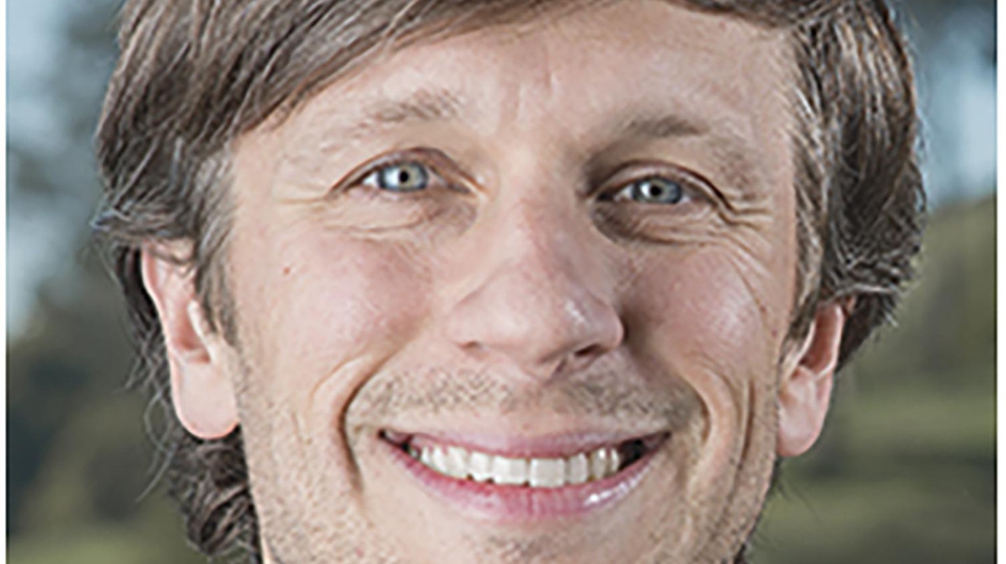
Imaging Atomic Structure, Strain, and Disorder By Atomic Electron Tomography

Event details
| Date | 10.07.2024 |
| Hour | 17:00 › 18:00 |
| Speaker | Dr. Peter Ercius | Lawrence Berkeley National Laboratory, Molecular Foundry, USA |
| Location | Online |
| Category | Conferences - Seminars |
| Event Language | English |
Knowledge of the atomic structure of materials is critical to understanding their functionality in many fields such as biology, microelectronics, condensed matter, and nanotechnology. Scanning transmission electron microscopy (STEM) is an effective method for measuring the atomic structure of materials based on so-called Z-contrast where the image intensities are proportional to the atomic number of the material being imaged. However, by its nature STEM is limited to producing only two-dimensional projections of a structure. Electron tomography is a technique that can reconstruct the three-dimensional structure of unique nanoscale objects from a series of two-dimensional images acquired at different viewing angles. Utilizing the sub-Angstrom real-space resolution of STEM with advanced tomographic reconstruction algorithms we have extended tomography to atomic resolution to solve the structure of materials at the single atom level without averaging or the assumption of crystallinity. This talk will present the abilities of AET to reconstruct order and disorder in materials with 20 picometer precision. Our success in resolving chemical order/disorder in metallic FePt nanoparticles was extended to include the time domain by capturing nucleation and growth or ordered phases in the same nanoparticle. Also, the ability to reconstruct atomic structure without the need for averaging or crystallinity led to the achievement of directly imaging three-dimensional atomic arrangements in amorphous solids. AET has become an important technique in the field of atomic structural characterization.
Biography
Peter Ercius graduated from Cornell University with a B.S. in applied and engineering physics in 2003. He remained at Cornell and completed a Ph.D. in applied and engineering physics with Professor David A. Muller in 2009. His dissertation project focused on three-dimensional (3D) electron tomography of semiconductor devices using scanning transmission electron microscopy (STEM). He then joined the NCEM facility as a collaborative postdoctoral researcher for 2 years before being hired as a permanent Staff Scientist of the Molecular Foundry. Peter is currently in charge of the electron tomography program at NCEM and the dual aberration-corrected TEAM 0.5. Dr. Ercius is a leading expert in electron tomography and collaborates with users of the Molecular Foundry on a wide range of projects including S/TEM atomic resolution imaging, electron tomography, 4D-STEM scanning diffraction, in situ liquid TEM, electron energy loss spectroscopy (EELS), and automated experimentation.
Practical information
- General public
- Free
- This event is internal
Organizer
- CIME